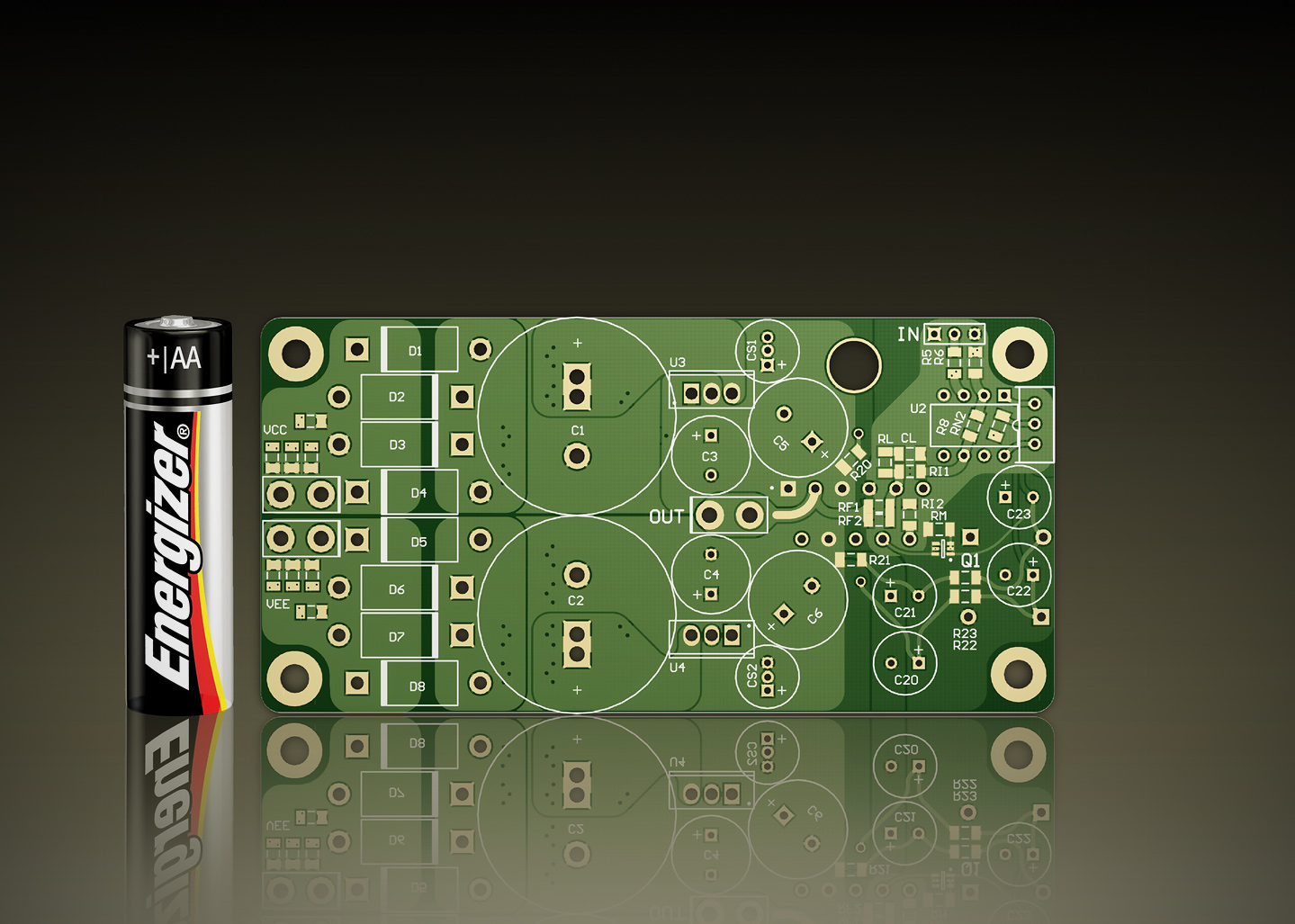
Release!
Schematics:
LM3886v8.pdf
7th...
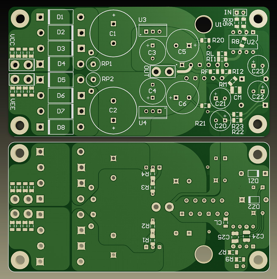
Schematics:
LM3886v7.pdf
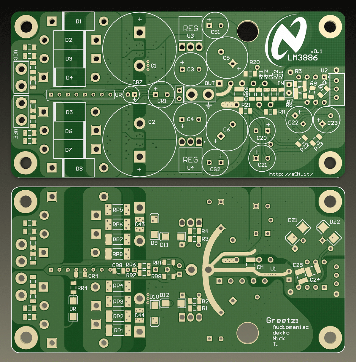
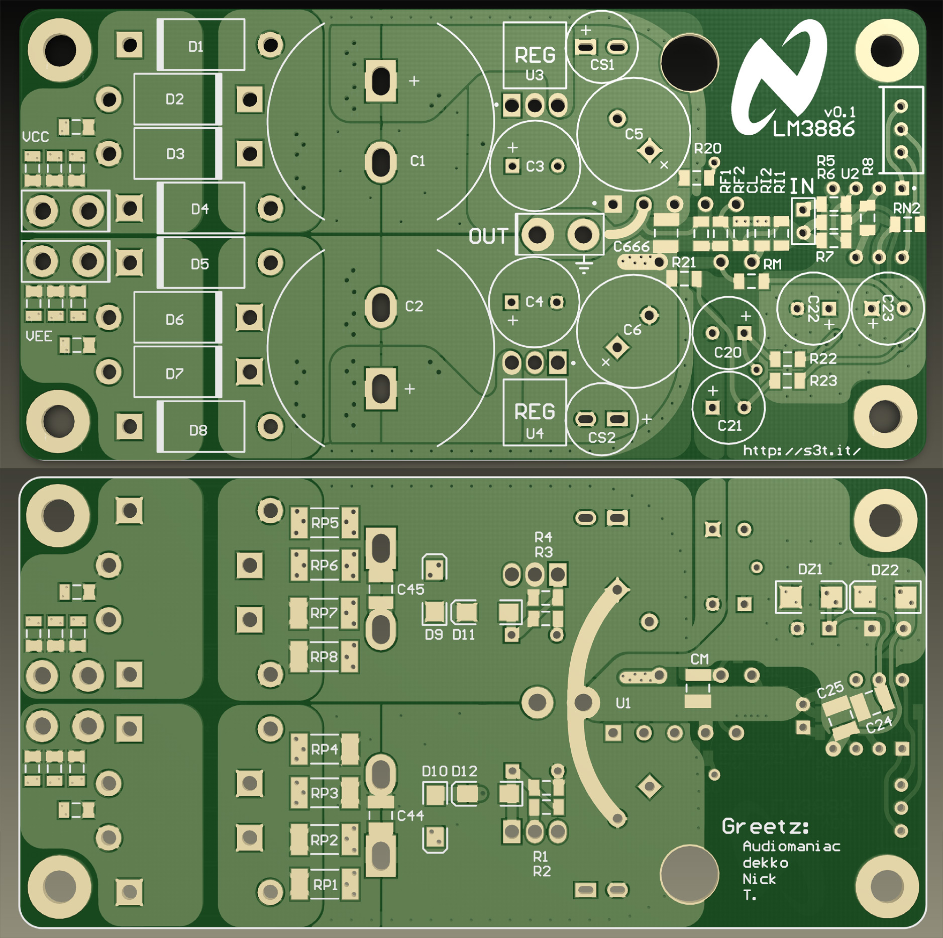
- Speaker DC offset protection, turn-on delay, quick turn-off by upc1237.
- Redone the plane cuts around PS caps
- Moved the trimpot next to the OpAmp's trim pins - less noise pickup.
- GND shielding of LM3886 case
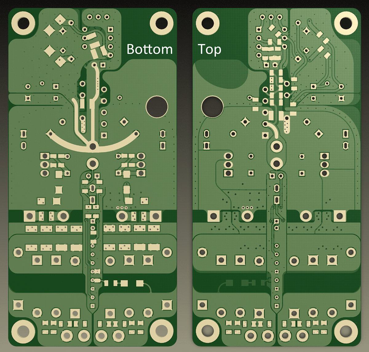
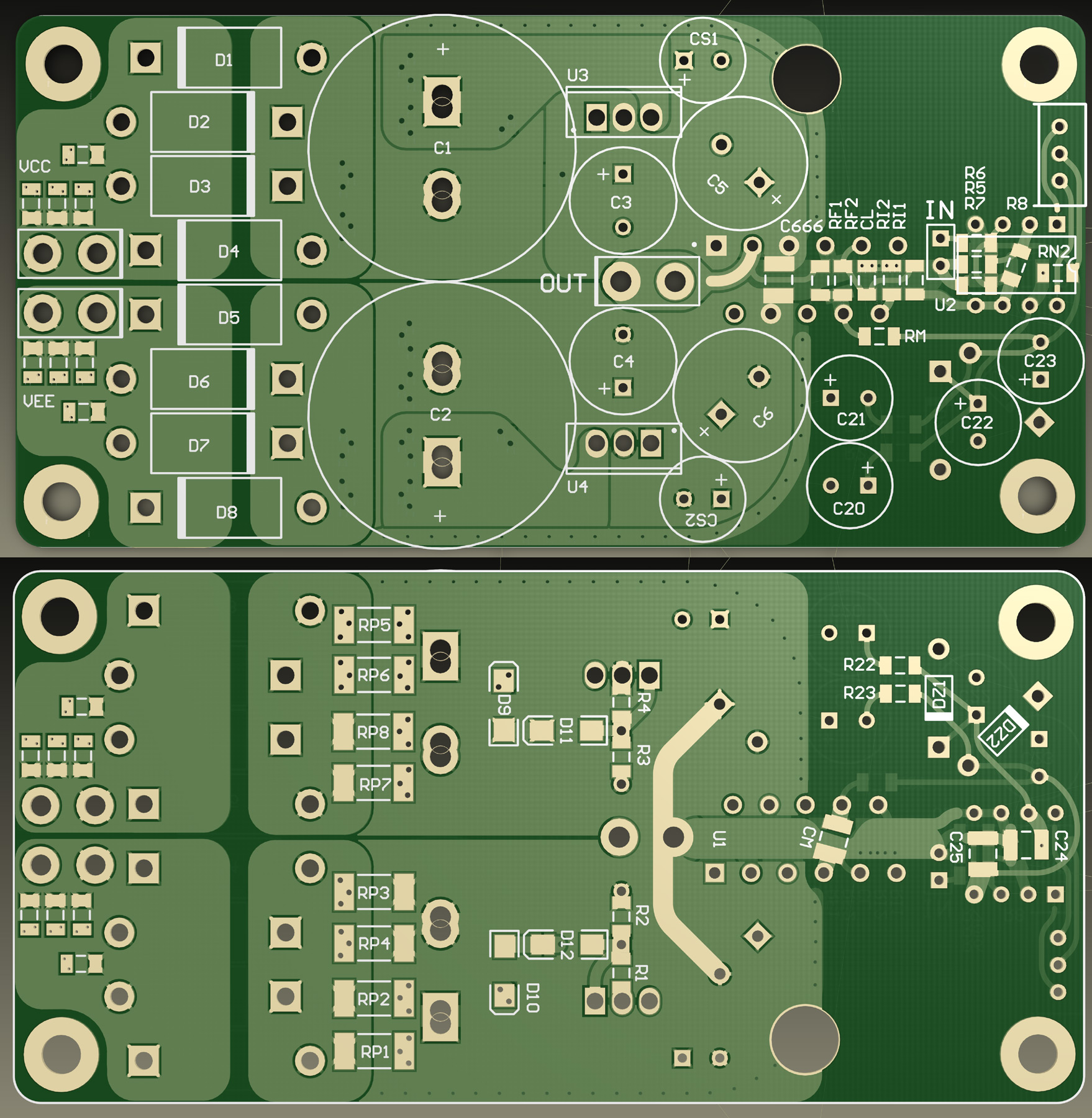
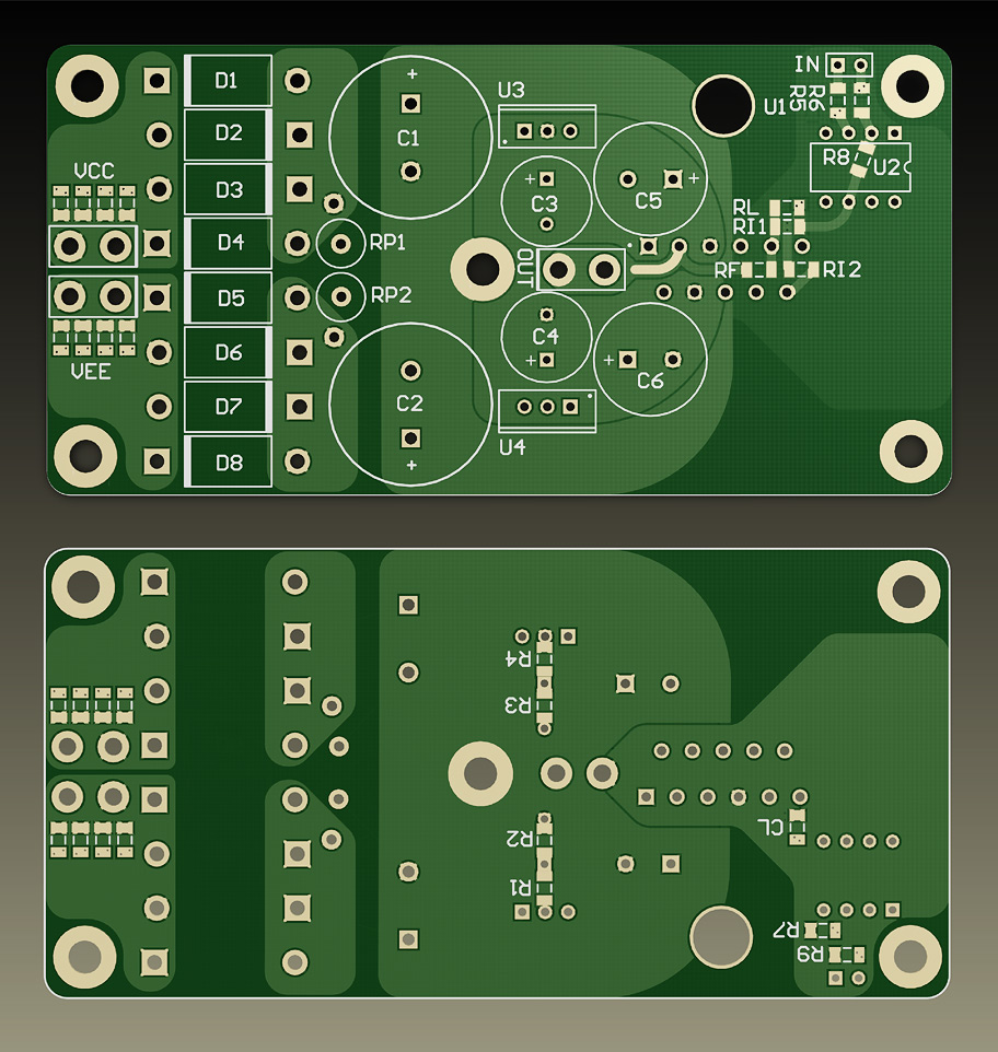
6th :)
- Gone with SMT zeners in input "preamp" circuit.
- Large pad for VEE - to make the LM's VEE pin thickier and lower impedance.
- Oval-shaped pads for the caps to accomodate different footprint sizes...
- Ground cut to force the current flow thru pins of PS caps
- Artwork as promised :)
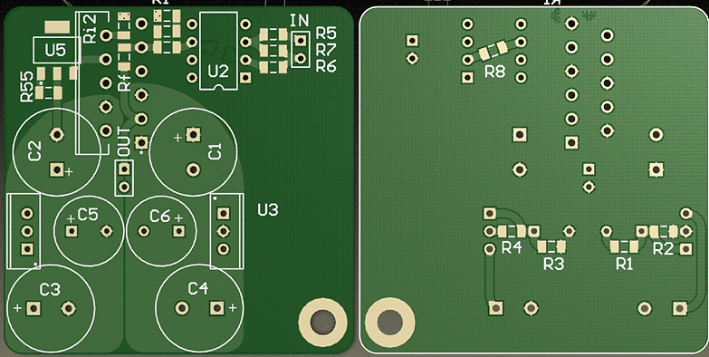
5th version...
- Series connected feedback resistors, "U" shape - to overcome heat gradient and thermal volage effect introduced by temperature gradient over feedback resistor.
- All the "input" resistors are in paralel, so the same temperature gradient will cause the same voltage developed on these resistors and will be eliminated by differntial opamp inputs. Hopefully the "noise" induced on these resistors will be eliminated too, as the resistors are close together - the noise will be common mode and the same direction, so opamp's input will just substract it.
- A shield around supply planes to the GND plane - hopefully will control EMI from PS rails
- Really short ground trace from input to output should help too, by reducing EMI pickup loop as well as less resistive traces.
- 1uF X7R 100v 1210 cap across the rails, right between PS pins of LM. Should kill some hi-frequency noise between the rails. Shortest path for these currents... Less ground pollution where electrolytics/regulators don't really work. Optional, but... Had to try it.
- Top-right corner is empty now... for some artwork!
4th version:
- Large (25mm) PS caps
- Series R after diodes - less switching noise, "soft" rectification. Not to mention the shottkys...
- GND split between PS rails...
- "0" trimpot
- Better place for mute cap (right next to the LM's GND pin which i guess is Mute's reference).
- Another ground slice between "preamp's" PS and signal ground.
- Guard diodes for LM338s
- Still in the 50x100mm (2"x4") package.
4v Schematics, disregard component values.
3rd version:
Polygons around the PS diodes/caps, PS for "preamp" stage, a bit of cutouts, fixed some layout bugs - 3D modeling of Altium helps to layout the mechanics stuff... nothing exotic.
2nd version. Not that "u" anymore... Gone with all-in-all solution, as the use of LM338 "negative" regs require separate windings/trafos for each amplifier. Hence the onboard diode bridge/PS caps.
Since I'm going with separate trafos, lower currents, rather low voltages, regulated... I could stick to Schottky diodes, add some resistance to the PS to tame that diode ringing even futher with RC filtering, some snubbering on trafo inputs...
Looks promising, but i need to redo the electromagnetics course to be sure everything is okay with magnetic fields (these are utter important in amplifier topology design - with high currents, high frequency, and extremely low noise on the input).
50x100mm (2"x4") board.
1st version:
 Schematics - v1
References:
Schematics - v1
References:
The thing is based on developments of:
- Audiomaniac and his Amp.01 amplifier (
http://www.audiomaniac.net/project/3-lm3886 )
- Dekko (
thread on vegalab.ru )
- Nick's ZD-50 (
http://www.s-audio.com/ )
and their design considerations.
Yet, disclaimer:
I tried to put the things that work in other designs together, yet in the scope of "small low-power amplifier" that looks like a regular line-level device - regulation, low voltages, extra bypasses et cetera.
Everything here should work at it's limits. 6800uF caps are almost-too-small, LM338 in TO220 is almost too weak, diodes are 40v schottkeys - again, on the limit of acceptance, as well as the RCRC and bypass networks with their power dissipation limits. 10k in the feedback is on the edge of power dissipation... Use of unbuffered LME into 3k load is on the edge too.
The most effort i've put into this amplifier is the layout, which, in my belief, is the most important thing as long as the schematics is OK. Keeping the large currents and their EM fields separate from input stage, keeping the input stage immune to EM fields et cetera... that's where the most effort gone to.