Work in progress: TDA1541A PCB layout.
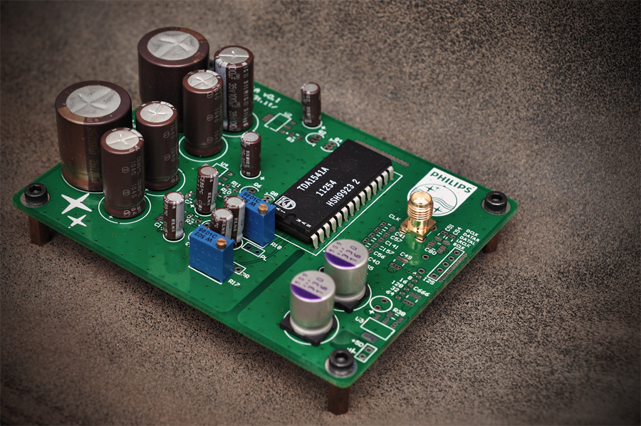 What do we have here?
- 5-stage CRC filtering for power supplies
- Classic LM317/337 pre-regulators with additional shunt-style transistor regulator/filtering per Nazar's
article.
- Ferrite beads everywhere on power supplies to suppress EMI in/out of the board.
- Reclocking circuit with 74HC175 - differential D-FlipFlop equally loaded to suppress ground/PSU bounce and keep it quiet.
- DEM clocking with single "differential" D-FlipFlop drive. On-board counter to divide BCLK rate down to required by DEM frequency - to liniarize Dynamic Element Matching behaviour.
- Filtering/level matching of DEM/I2S lines - to reduce the digital switching noise leakage to DAC IC.
- SMA CLK input for reclock circuitry - impedance matched/controlled clock input for better jitter performance.
- X7R 1206 4.7uF DEM decoupling capacitors - better suppression of DEM switching/averaging.
- 2mA additional bias on analog outputs to get zero-centered current output out of the DAC for proper integration with various I/V stages and to stay away off DAC's voltage compliance level.
- Filtering of analog outputs to suppress sample switching introduced glitches directly at the source of the switching - shortest return path of switching currents.
- Low impedance I2S connector/ribbon cable for lowest possible EMI. Additional ferrite common mode choke (EMI filter) is welcome here too.
- Top layer is mostly GND - to shield the traces from EMI, and to lock the traces between this GND layer and chassis.
- Additional shielding could be soldered on top of digital side to futher reduce the EMI.
- Accepts both I2S and paralel (simultaneous) data input.
- Accepts external DEM CLK input.
- Possibility to operate without dem clock - in the classic way with DEM clk capacitor.
Schematics:
http://s3t.it/data/uploads/tda1541_v014.pdf
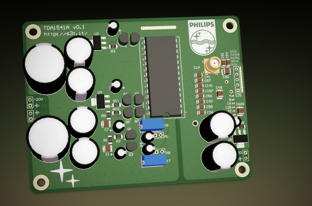
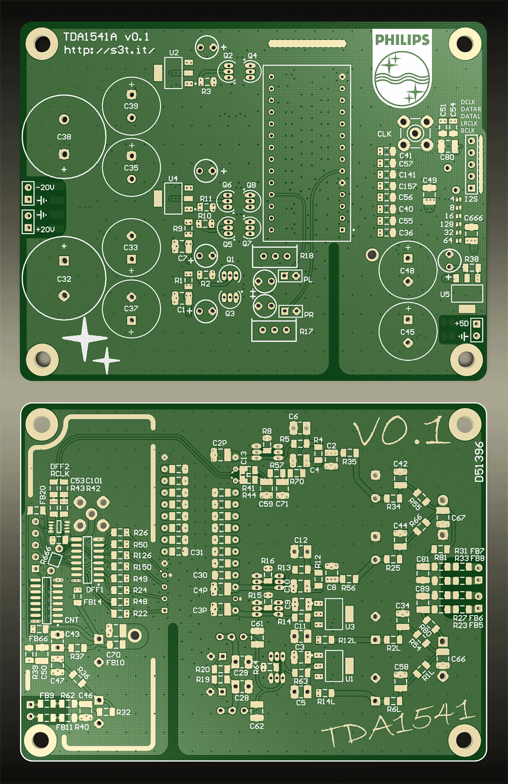
Probabply release candidate:
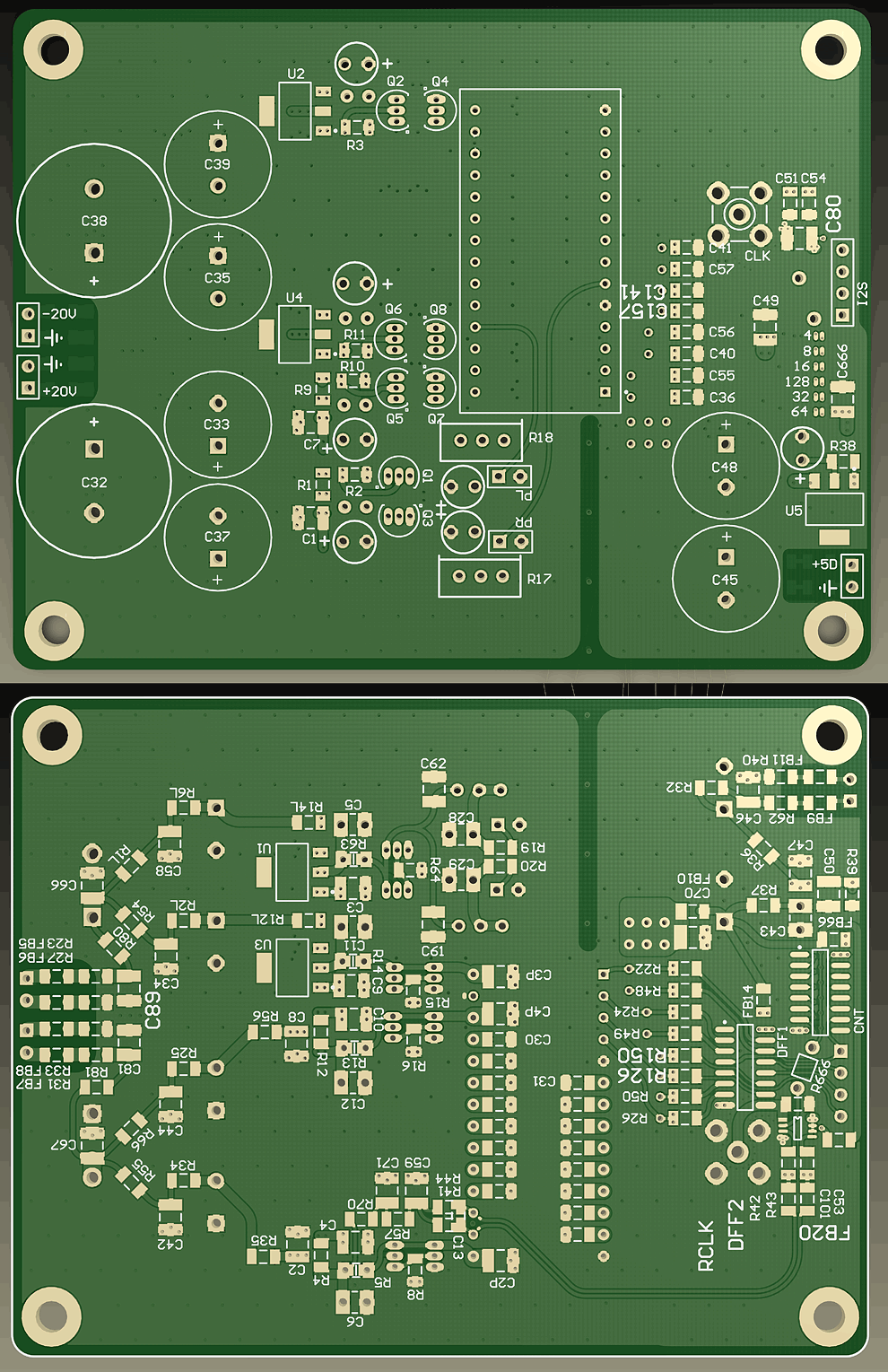
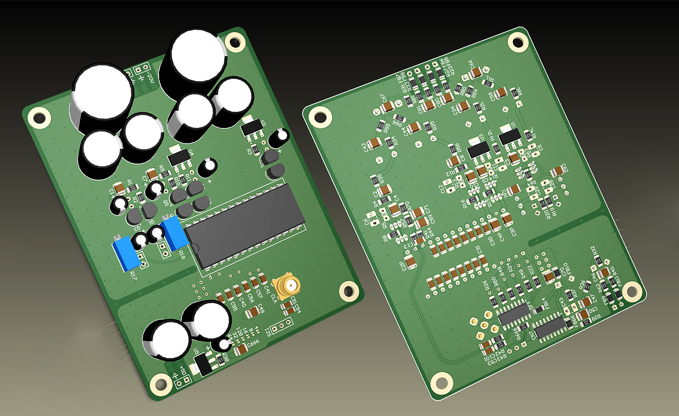
Rev. 0000 thru rev. 0003:
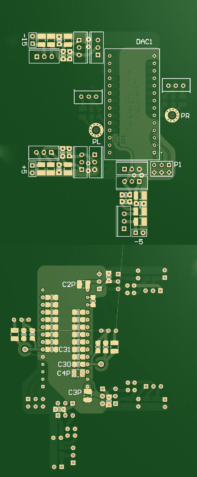
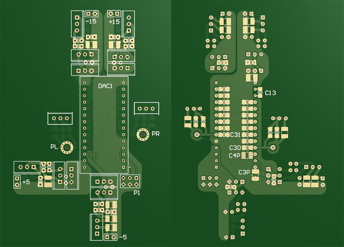
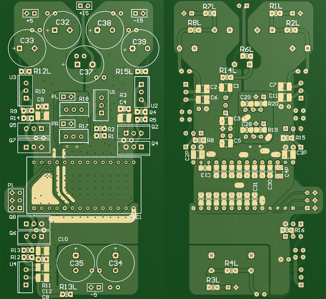
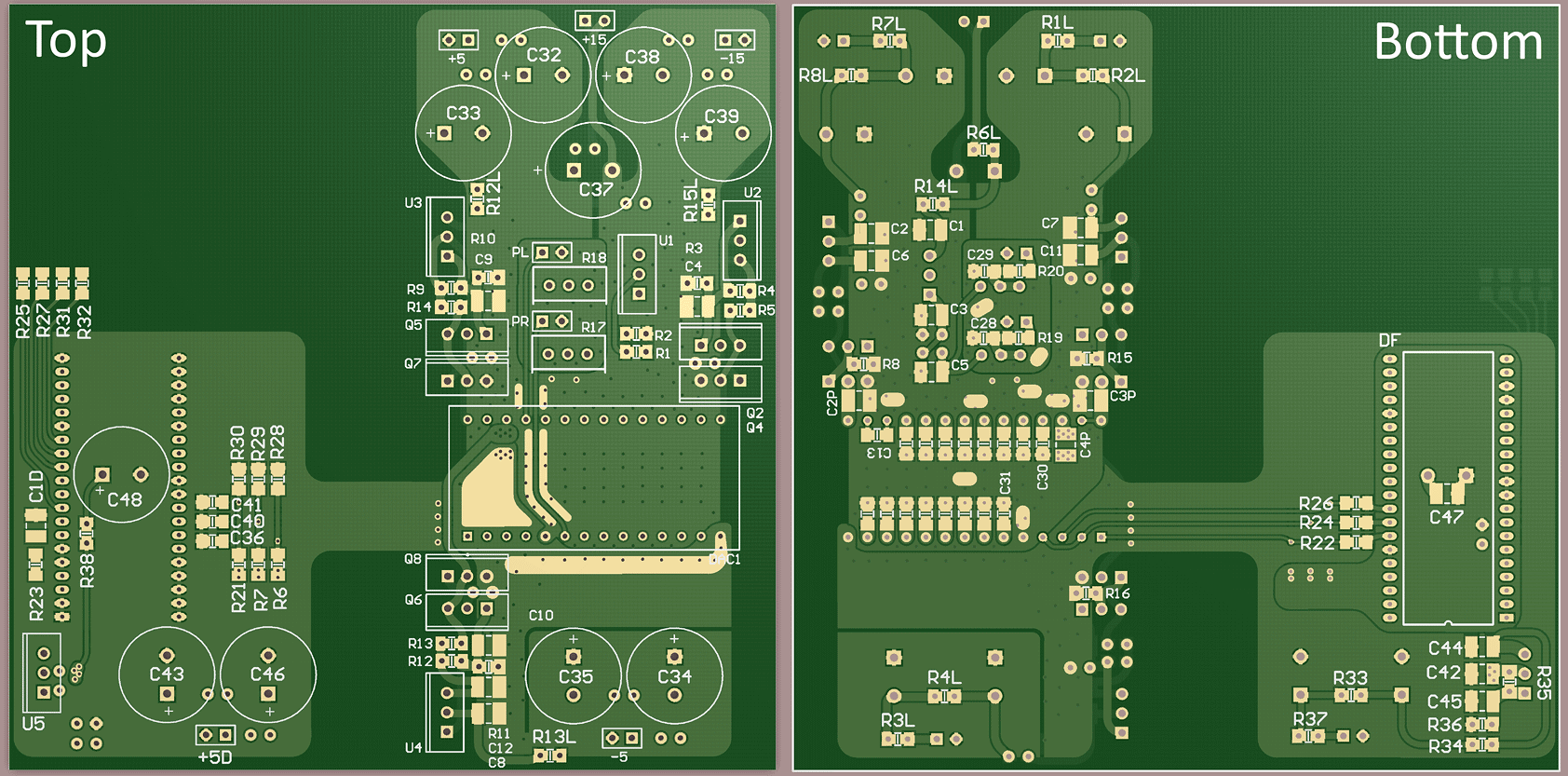
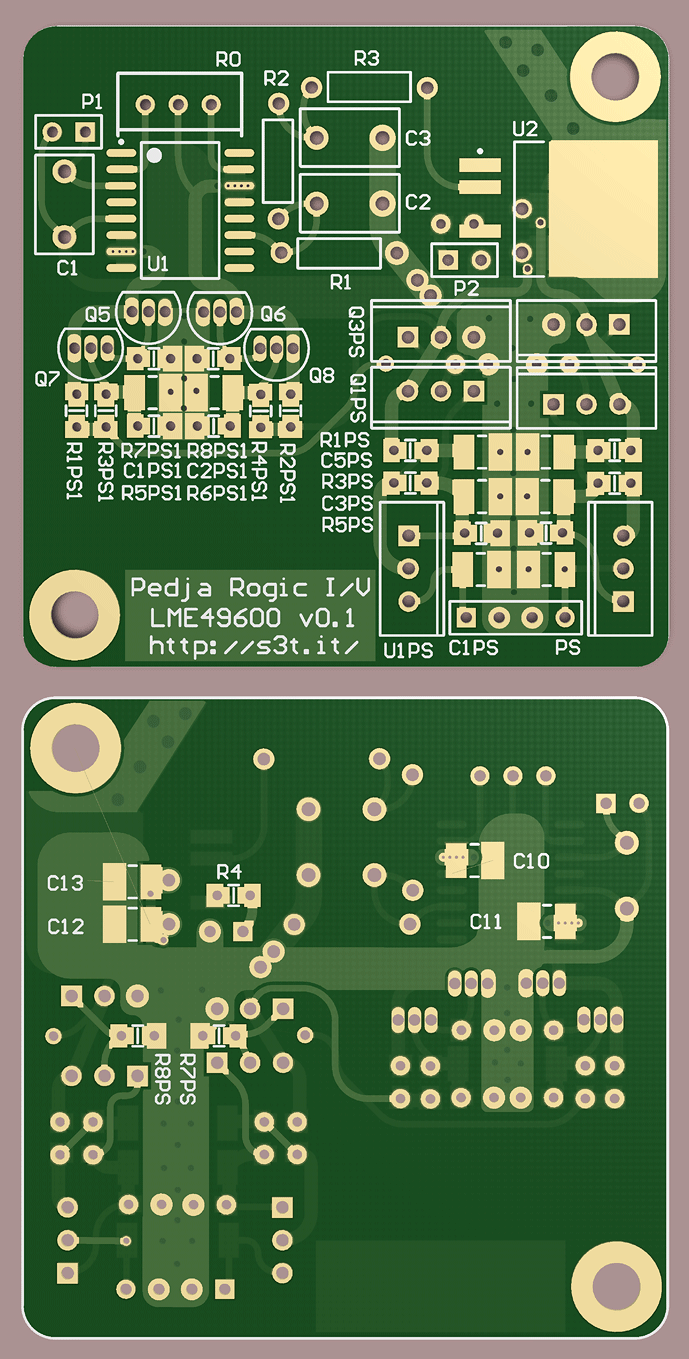
And the output stage:
There will be 2 (or even more) versions, with LME49600 and LH0033 buffers.
And maybe the
discrete I/V from Pedja too.
